Fig. 4
Complete
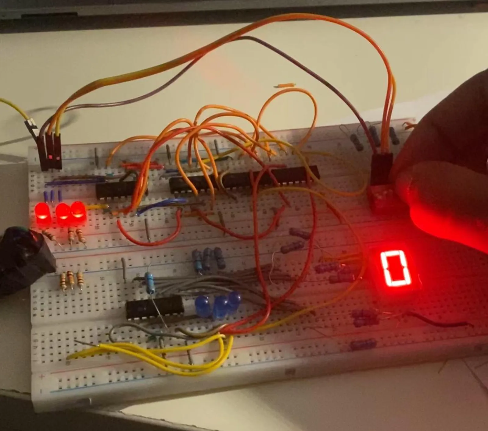
3-Bit Encryption/Decryption Circuit
A hand-picked substitution cipher, reduced to nothing but NAND gates
A pair of combinational circuits for Digital Logic Design: one maps every 3-bit value to a different one under a fixed substitution, the other undoes it exactly. Each was designed from its own truth table, minimized with Karnaugh maps, then redrawn in NAND-only form — the project's one hardware constraint — and wired on breadboards with 4011 and 7410 NAND ICs, DIP switches for input, and a 74LS47 driving a 7-segment display per circuit.
Plates
1 plate
-
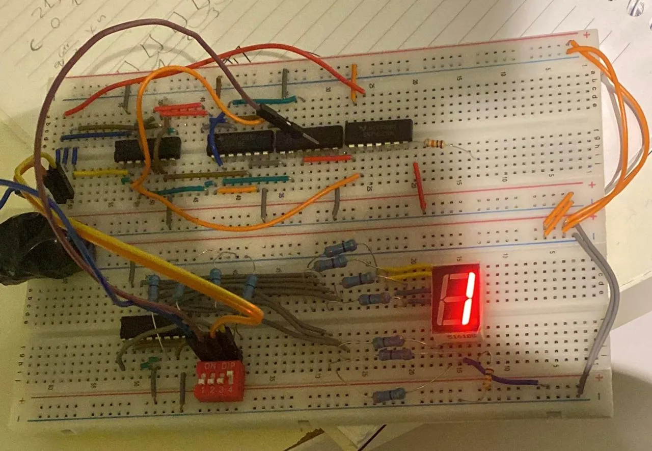
Plate 1 — The full board: DIP switches set A, B, C by hand; the display shows the circuit's current output.
Procedure
3 min
What it does
Two circuits, each taking a 3-bit value (A, B, C — one of eight) and producing a different 3-bit value (W, X, Y). The first encrypts: every input maps to a different output, so nothing encrypts to itself. The second decrypts: it takes that circuit’s output and reproduces the original input, exactly.
The project’s one rule on the hardware: however the logic came out, it had to be rebuilt from nothing but NAND gates.
Picking the cipher
The only constraint on the substitution itself was that no value encrypt to itself. The mapping chosen here turns out to be a single eight-element cycle: 0 → 6 → 5 → 2 → 4 → 1 → 3 → 7 → 0. Run a value through encryption eight times in a row and it comes back to where it started; run it through decryption once and it undoes exactly one step of that cycle.
Truth table to Karnaugh map to NAND
Each output got the usual three-pass treatment: write the truth table straight from the chosen mapping, read a minimized sum-of-products off a Karnaugh map, then apply De Morgan’s theorem until every gate in the expression was a NAND. Decryption wasn’t derived algebraically from encryption — it got its own truth table (the same eight rows, input and output columns swapped) and its own independent minimization.
| Encryption | Decryption | |
|---|---|---|
| First bit | W = A’C’ + A’B + BC’ | A = W’Y’ + X’Y |
| Second bit | X = A’B’ + A’C + B’C | B = X’Y’ + WY |
| Third bit | Y = AC’ + A’C | C = W’Y’ + XY |
Built on the breadboard
Two NAND IC families supplied every gate: the 4011 (quad 2-input NAND) for two-input terms, the 7410 (triple 3-input NAND) for the three-input ones. A 74LS47 BCD-to-seven-segment decoder drives a display per circuit from its 3-bit output — wired into the low three bits of the 74LS47’s 4-bit BCD input — through a 330 Ω resistor on each segment. A 4-way DIP switch sets A, B, C by hand.